
Prof. Alferov has attended the Lindau Meeting in 2001. Due to the rotation of disciplines the Laureates will be invited every three years. The 2nd interdisciplinary Meeting was held in 2005.
Zhores Ivanovich ALFEROV was born in Vitebsk, Byelorussia, USSR on March 15, 1930. In 1947, he graduated from high school (Minsk, Byelorussia) and in 1952, he graduated from the Department of Electronics of V.I. Ulyanov (Lenin) Electrotechnical Institute in Leningrad. Since 1953 until now he has been a member of the Scientific staff of the Ioffe Physico-Technical Institute of the Russian Academy of Sciences where he consequently held the following positions: junior scientist (1953- 1964), senior scientist (1964-1967), Head of Laboratory (1967-1987), Director of the Institute (1987 - present). He received two scientific degrees: a candidate of science in technology in 1961 and a doctor of science in physics and mathematics in 1970 - both from Ioffe Institute. In 1970-1971 he spent 6 months as a visiting scientist at the University of Illinois, USA. Since 1962 he has been working in the area of III-V semiconductor heterostructures. His outstanding contributions to physics and technology of III-V semiconductor heterostructures, especially injection properties, development of lasers, solar cells, LED’s, epitaxy processes have been led to the creation of modern Heterostructure Physics and Electronics. For his achievements in this area Prof. Zh.I. Alferov was honored with many Soviet, Russian and International awards, and honorary memberships. In 1990, Zh.I. Alferov was elected a Vice-President of the Academy of Sciences of the USSR. In 1991 he was elected a Vice-President of the Russian Academy of Sciences and President of the St.Petersburg Scientific Center of the Russian Academy of Sciences. The Ioffe Institute: 2300 employees (1100 researches).
Most important Awards:
Franklin Institute Ballantyne Medal (USA, 1971); Lenin Prize (USSR, 1972); Hewlett-Paccard Europhysics Prize (1978); State Prize (USSR, 1984); Award & Heinrich Welker Medal of the International Symposium on GaAs and Related compounds (1987); A.P. Karpinskii Prize (FRG, 1989); A.F. Ioffe Prize (Russian Academy of Sciences, 1996); Demidov Prize (Russian Federation, 1999); A.S. Popov Medal (Russian Academy of Sciences, 2000); Nick Holonyak Jr. Award (Optical Society of America, 2000); Nobel Laureate in Physics (2000).
USSR Orders:
The Badge of Honour (1959); Order of the Red Banner of Labour (1975); the Order of October Revolution (1980); Order of Lenin (1986) and 3 Medals.
Russian Federation Orders:
“For Merits to Fatherland” III degree (1999); “For Merits to Fatherland” II degree (2000) and 3 Medals. Orders and Medals of the different Russian Scientific and Social Societies.
Most important memberships:
Zh.I. Alferov is a full member (Academician) of the Russian Academy of Sciences (1979); Life Fellow of the Franklin Institute (U.S.A., 1971); Foreign Member of the Polish Academy of Sciences (1988); Foreign Associate of the National Academy of Engineering (U.S.A., 1990) and Foreign Associate of the National Academy of Sciences (U.S.A., 1990); Foreign Member of the National Academy of Sciences of Belarus (1995); Honorary Foreign Member of the Korean Academy of Science and Technology (1995); Honorary Doctor of the Kurchatov Institute (Moscow, 1998); Foreign Member of the National Academy of Sciences (Ukraine, 2000); Honorary Professor of the State Technical University (St.-Petersburg, 2000); A Fellow of the Optical Society of America (USA, 2000); Honorary Professor of the State Electrotechnical University (LETI) (St.-Petersburg, 2001); Honorary Professor of the Moscow State University (Moscow, 2001).
He is a Member of the Committee of Science and Education of the State Duma (1995 - present). Zh.I. Alferov has 3 books, more than 500 scholarly publications and 50 Inventions in Semiconductor Technology.
Avocation: swimming, cross country skiing and the history of World War II.
Prof. Alferov passed away on 1 March 2019, at the age of 88.
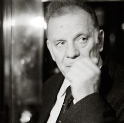
This text and the picture of the Nobel Laureate were taken from the book: "NOBELS. Nobel Laureates photographed by Peter Badge" (WILEY-VCH, 2008).
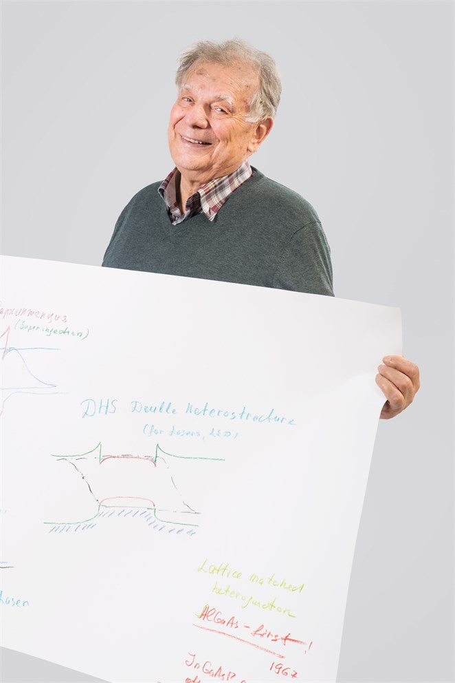
Exhibition "Sketches of Science" by Volker Steger - Locations & Dates
Solid State Engineering
by Adam Smith
“I didn’t anticipate it,” recalls Zhores Alferov. “I was thinking that there only would be photographs, but when he came to my country house, he proposed to me to draw something about the problems for heterostructures for which I was getting Nobel Prize! And I was just writing some important physical phenomena and applications. I mention in this picture just some applications: for lasers and some physical phenomena which I called superinjection heterostructures.”
Alferov and his fellow Laureate Herbert Kroemer were awarded one half of the Nobel Prize in Physics in 2000 for their independent creation of new semiconductors with novel properties, materials that revolutionised solid state physics and now form the basis of modern communications and information technology. Mixing different semiconductors into ‘heterostructures’ allowed them to engineer changes in electrical conductivity, giving rise to previously unseen quantum phenomena. “By the creation of very complicated compositions of different materials with very thin layers, you create material properties which do not exist in nature,” explains Alferov. He recalls that his friend Leo Esaki, also a Nobel Laureate, once remarked that these heterostructures are ‘man-made crystals’, in contrast to all other materials which he called ‘God-made crystals’.
The sketch introduces some of the concepts associated with Alferov’s discoveries. At the bottom right is a reference to two semiconductors; aluminium gallium arsenide (AlGaAs) and indium gallium arsenide (InGaAs). Above these, the word ‘heterojunction’ refers to the engineered interfaces between different semiconductors. It is the change in the allowed energy levels of electrons as they cross these junctions that give rise to heterostructures’ unique properties. Such changes in energy bands are depicted in the diagrams. In the centre, for instance, so-called ‘electron and optical confinement’ is illustrated for a double heterostructure (DHS), a sort of semiconductor sandwich now used widely in optoelectronics.
“When we started our research in the middle of the 60s,” says Alferov, “It was just a few laboratories in the world. That’s all. Now, it’s hundreds of laboratories all over the world. At any conference in semiconductor physics, practically 60-70% of talks are connected with heterostructures. So I am very happy that I started that research early and got important results … I am happy man!”